Introduction:
Transport properties of two-dimensional electron gas systems (2DEG) in double quantum wells are the subject of intensive and diverse investigations. If the length scales in such structures are small enough that the electron waves preserve their phase coherence, quantum-effect devices which utilize coherent electron waves can be realized. Major advantages of such devices should be a very low power consumption and high switching speed. Coherent resonant tunnelling, for example, can be used to build an electron wave switch[1,2]. In such a device two quantum wires (electron waveguides) are closely adjacent, separated by a thin barrier, forming a double quantum wire structure. When the barrier is reduced, the two electron waveguides will be coupled and the electron wave will oscillate between the two waveguides. If the length of the coupling region corresponds to half an oscillation period, the electrons can be transferred from one waveguide into the other, thus forming an electron wave switch.
Vertically Stacked Electron Wave Switch:
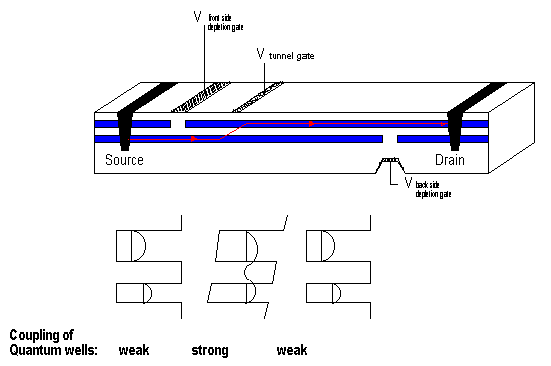
In a vertically stacked electron wave switch two quantum wells of different thickness are closely adjacent, separated by a thin barrier, forming a double quantum well structure[3]. Due to the different thickness, the energies of quantized states in these 2 wells do not line up. Applying a voltage to a gate electrode on top of the device can be used to line up the energies of occupied states. As long as the coherence of the electron waves is guaranteed, coherent resonant tunnelling between two 2DEG´s can take place. In these structures, the tunnelling barrier is realized by epitaxy, which leads to a small, well defined barrier. Furthermore, applying a voltage to the tunnel-gate does not influence the width of the wires, or the number of modes in the electron wave guides, as is the case for the split gate structures.
 Normally both 2DEG´s are contacted simultaneously, because in double quantum well structures the wells must be very closely adjacent to observe coherent electron wave properties. For that reason most measurements are restricted to parallel transport properties. If coherent resonant tunnelling between two 2DEG´s is to be investigated, both 2DEG´s must be contacted independently, though. Realizing such independent contacts is therefore a major task. Eisenstein et al.[4] realized these structures by using ohmic contacts to both 2DEG´s and than selectively depleting the 2DEG´s with gate electrodes on the front and back side of the device. Until now such devices based on the AlGaAs/GaAs material system have been investigated.
Our aim is to realize and investigate coherent resonant tunnelling between two 2DEG´s based on the InAlAs/InGaAs/InP material system. This material system generally possesses many advantageous characteristics compared to the AlGaAs/GaAs material system.
References:
[1] J.A. del Alamo, and C.C. Euster, Appl. Phys. Lett. 56, 78 (1990)
[2] N. Tsukuda, A.D. Wieck, and K.Ploog, Appl. Phys. Lett. 56, 2527 (1990)
[3] H. Sakakibara, M. Noguchi, T.J. Thornton, K. Hirakawa, and T. Ikoma, IEDM93 Tech.. Digest 44 (1993)
[4] J.P. Eisenstein, L.N. Pfeiffer, and K.W. West, Appl. Phys. Lett. 57, 2324 (1990)
[5] S. Sen, F. Capasso, A.L. Hutchinson and A.Y. Cho, Electron. Lett. 23, 1229, (1987)